Coating Capabilities
Custom Design & Engineering
The ZC&R Coatings for Optics (ZC&R) team of design and manufacturing engineers collaborate with our customers to understand their wholistic market and application needs. This synergistic approach allows us to develop innovative thin film coating solutions to better meet their market and photonics enabled application demands. ZC&R customers gain access to innovative solutions unavailable elsewhere due to Abrisa Technologies’ expertise in a multitude of market applications, technical knowledge from fields of optics, physics, thin films, mechanical engineering, electronics, semiconductor, material properties, and of course our experience with designing thousands of thin film solutions. Couple this with volume manufacturing experience for both technology glass and thin film coating for a Total Solution approach.
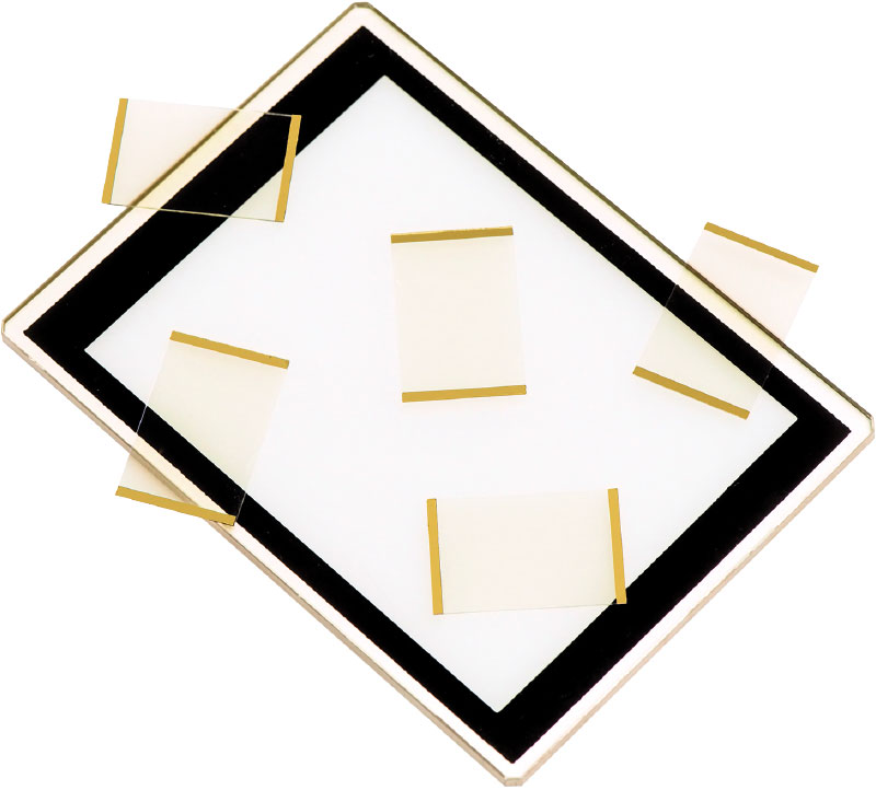
- Thin Film design, solutions and applications engineering and program management
- Designs from 200nm to 20 microns
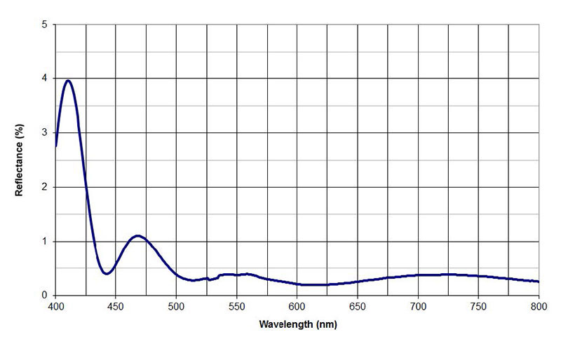
- Anti-reflection, reflecting/mirrors, partial transmission and beam splitters, filters, color and correction, dichroics and edge filters, selective attenuation and absorption, selective signal, lasers, transparent conductive, heat and temperature management, EMI shielding, LC-switch, defense applications, lighting, and more.
- Optical coating solutions with additional fitness-for-use enhancements
- Damage resistance, bio/chem compatibility, thermal resilience, transparent conductivity, electrical isolation, outdoor use, oleo/hydrophobicity, and more.
- Designs for volume manufacturability, repeatability and predictable results
- Thin film modeling design software calibrated to match our deposition processes, combined with manufacturing know-how and process monitoring controls.
- Thousands of existing design solutions or new solutions tailored to your application
- Experience with special process qualification, process lock, and validation
- Semiconductor, defense, avionics, medical, dental, telecom, and automotive
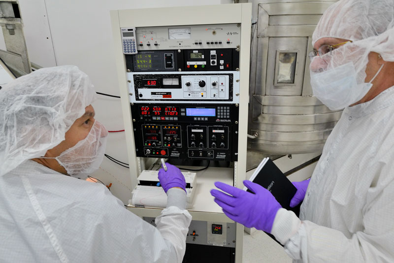
Coating Chambers
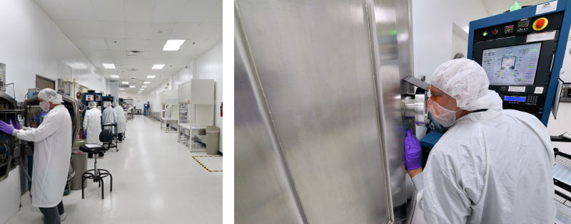 ZC&R’s coating facility has large volume coating capacity with a 3-shift operation and redundant large e-beam chambers with available Ion Assisted Deposition (IAD), supporting volume and large part production needs for dielectric and metal coating materials. Medium to large chambers range from 32 to 72” diameter. Additional smaller chambers are available to support prototyping, smaller part and smaller batch coating needs. Our parent, HEF, manufactures its own PVD coating chambers and continues to invest in expanding our coating capacity and giving our customers access to other PVD deposition technologies (sputtering) to support their growing needs and technology roadmaps.
- Chamber sizes for flexible manufacturing – 32” (813mm) to 72” (1830mm) diameter
- Precision Controlled deposition monitoring techniques
- Combination of narrowband/broadband optical and crystal quartz monitoring
- Ion-Assisted deposition (IAD) for durable hard coatings
- Available for: 32” (813mm), 48” (1219mm), 64” (1626mm) and 72” (1830mm)
- Specialty coating processes for extra high density and autoclavable coatings
- Competitive advantage using coat then fabricate process – (4) diameter/run
- Large 23.5”, 24”, or 27” diameter substrates are handled more efficiently and can be fabricated to size after coating. Tooling for substrates to 29” in diameter
Substrates, Size & Shape Specifications
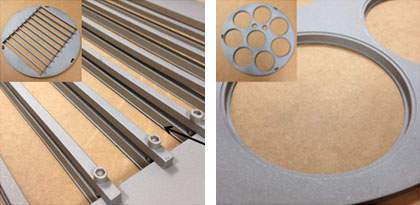 ZC&R coats materials of many shapes and sizes from 2.5mm to 27” with thicknesses from 0.070mm to 6.0”, and accommodates coating formats that are miniature, ultra-thin, unusually shaped, needing contiguous surface coating, require minimal tooling marks or pattern registration. Customers can take advantage of our economical coat then fabricate process using our 24” and 27” diameter formats or utilize our highly efficient semi-format wafer and filter glass tooling, or prototype with our flexible adjustable rail tooling with no NRE tooling investment. We have available in-house custom tooling design capability for unusual part shapes, heavy loads, or high volumes per batch needs.
- Sizes: From 0.1” (2.54mm) to 27” (686mm) diameter, custom up to 36” (914mm) diameter
- Thicknesses: From 70 microns up to 6” (152.4mm)
- Formats: Large rounds, flats, blocks, wedges, lenses, fibers, cylindrical (external), custom
- Tooling Accommodation:
- Tooling to hold 4 rounds of 24” and 27” per batch
- Adjustable Rail Tooling – accommodates up to 19”
- Standard Pocket Tooling for wafer and filter glass formats: 150mm & 200mm diameter, 6.0”, 6.5” and 7.0” square
- Custom Pocket Tooling for high volume batch coating, custom shapes, large clear apertures or patterned coatings with shadow masks
- Contiguous 3-surface edge coating (bus bars)
- Special tooling and masking
Substrate Materials Coated
ZC&R provides Total Solutions and thin film coating deposition services on a broad array of materials and continually adds new PVD coating capabilities and materials to its repertoire. Let us know what you are interested in.
- Glass: Float glass, borosilicates, fused silica, fused quartz, filter glass, AGC EN-A1, Corning® Eagle® XG, Corning® Willow®, SCHOTT Borofloat® 33, SCHOTT D263®
- HIE Aluminosilicates: AGC Dragontrail™, Corning® Gorilla® Glass, SCHOTT AS 87, SCHOTT Xensation®, chemically strengthened soda lime float, non-glare glass
- IR and special substrates: Silicon, germanium, zinc selenide, zinc sulfide, AMTIR, MgF2, sapphire, fluorides, polished ceramics, crystalline quartz
- Metals: Polished stainless steel, polished aluminum, titanium alloys
- Other: Other optical glass, select PMMA, Polycarbonate, and more
Measurement & Inspection
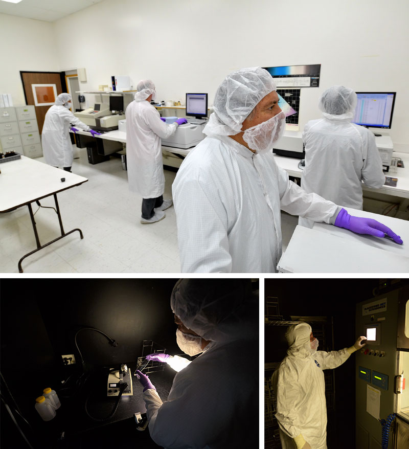 ZC&R utilizes a wide array of metrology tools and inspection processes, ensuring our coated Total Solutions perform as promised while consistently meeting our customers’ expectations. We welcome the opportunity to qualify coatings for use conditions in our environmental chamber, and subject them to adhesion, abrasion, and other testing. We are happy to entertain simulating customers’ inspection test set-ups to ensure they are receiving calibrated verification results.
- Spectrophotometers – Transmission and reflection measurement from 200nm up to 20µm at angles of incidence from 0 to 52 degrees
Four-point probes – Sheet resistance measurement for transparent conductive and metal coatings. Non-contact and bus to bus measurement available - Temperature/humidity chamber – In house environmental testing per MIL-C-675C and similar specifications to simulate use conditions
- Colorimetry – Precision measurement via spectrophotometer – for chromaticity/brightness, color temperature, color neutrality, and more
- Laser damage threshold – 3rd party testing via national and commercial facilities
- Abrasion and adhesion – performed per MIL-PRF-13830B and ISO Specifications
- Salt solubility (in-house) and salt fog (3rd party) – per MIL-C-14806A and similar
- Dust and fungus – performed per MIL-C-14806A (3rd party)
- Diffuse Reflectance – Special Testing for Display Glass
- Thermal Imaging for ITO Heater Heating Profiles
- Surface Quality – visual inspection with lighting/enhancement tools to 10-5
Patterning
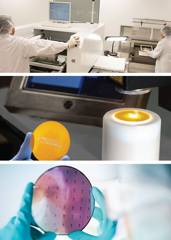
- Shadow Masking – ZC&R works with precision mask fabricators, creating custom shadow masks that are interposed between the coating and the substrates during deposition to selectively block coating being applied to certain areas of the substrate. Shadow masking is suitable for feature sizes down to 0.20″ (5.0 mm)
- Photolithography – Precision patterning and zonal coating achieved using photoresist and lift-off or etching between coating processes. Feature sizes from 5µm to 20µm can be achieved depending on the coating type required.
- Printed Etching – Printed etchants are typically used to selectively remove coating to expose conductive layers for electrical contact. A suite of printing systems are used to achieve feature sizes as fine as 0.030″ (.76mm). Printed etchants can also be utilized to remove all coated layers with a pattern size of 0.040″ (1.08 mm).
- Laser Marking – Select coatings, glass, and screen printed graphics can be patterned using an ablative CO2 marking process where non removeable part numbers and unique identifiers as QR codes or serial numbers can be added for traceability.
Ultrasonic & Other Cleaning
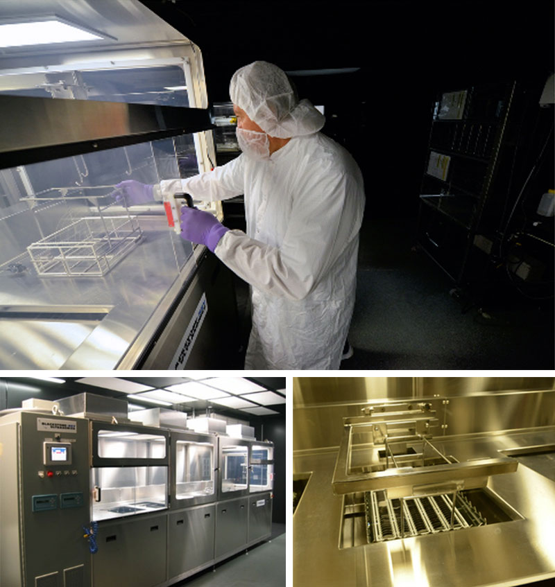 Good coating performance must start with good substrate quality including its cleanliness. All materials to be coated must be properly cleaned and pristine prior to coating. Substrates need to be free of contaminants, lubricants, particulates, organics, fingerprints and other foreign matter as particulates and contamination can lead to optical performance issues or degradation, coating adhesion problems, mechanical damage as well as reduced laser damage threshold. ZC&R employs several effective cleaning methods suitable for use on a wide range of optical materials and formats.
Methods used to clean and prepare substrates for coating include:
- Manual washing with cleaning solutions and tools appropriate for format and glass type
- Ultra-precision proprietary laser optics cleaning
- Special handling/cleaning processes for ultra-thin glass < 0.2mm
- Hands free automated ultrasonic cleaning system and vapor drying process for semi-format wafers and other sensitive parts requiring “non- contact” cleaning and particulate controls to the 10-5 level
- Cleanroom, special and multi-pack packaging also available upon request